|
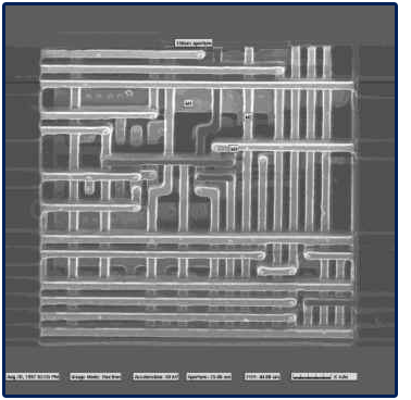
The image opposite demonstrates the effects of Gas Assisted Etching (GAE).
The image shows an integrated circuit that has been etched over a large area
using XeF2. By using GAE, the dielectric has been preferentially milled
with most of it being cleared away by the XeF2. XeF2 removes dielectrics at
a greatly enhanced rate compared to conventional milling, and allows a great
deal of dielectric to be removed with a minimum dose from the FIB's beam.
With a greatly reduced dose, the metal lines (for which milling is not
enhanced by the XeF2) show minimal sputter.
|
|


