|
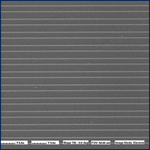
The location of an area of interest can be done using the FIB microscope's imaging capabilities. Imaging the sample allows the area of interest
to be selected visually. For semiconductor devices, the FIB system's precision navigation capabilities can be
employed to locate the region of interest with an accuracy that is on the order of microns. The image shows part
of a memory array structure of an integrated circuit from which a TEM "lift-out" specimen will be prepared.
|