|
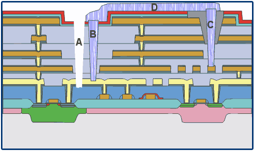
Below is a schematic showing graphically the capabilities of FIB Device Modification
(also known as 'Microsurgery' or 'Circuit Edit') on integrated circuits:
FIB milling using Gas Assisted Etching (GAE) is used to create a high aspect ratio hole through Metal 1. The GAE
increases the aspect ratio of the milled hole and improves "end-point detection," making it easier to recognize when
the desired metal line has been reached.
The FIB is then used to cut Metal 1, and then again to clean the area, ensuring that no stray material is left over from
the procedure, greatly reducing the possibility of shorts.
FIB milling with GAE to reach Metal 1 with good end-point detection.
The hole is then filled with conductive tungsten deposited by the FIB, creating a via to the surface.
FIB milling using GAE yields a high aspect ratio hole through the middle of Metals 5 and 4,
leaving sufficient metal in each layer to allow the lines to remain conductive.
The hole is then filled with FIB deposited Silicon Dioxide to insulate against shorts to Metals 5 and 4 from the
subsequent via that will be formed shortly.
The deposited Silicon Dioxide is then milled through using GAE and a high aspect ratio hole is opened down to Metal
2 with good end-point detection. GAE increases the rate of milling and improves the ability to recognize when you
have reached the desired metal line.
The high aspect ratio hole is then filled with FIB deposited tungsten, creating a conductive via all the way to the
surface.
The FIB is then used to lay down a well defined strap of tungsten across the surface of the device. This strap
connects the two vias that have been created.
|